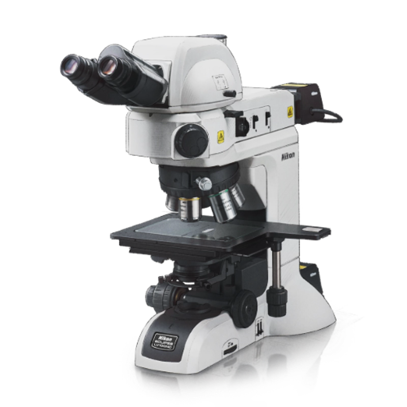
Nikon challenges ASML's lithography dominance with lower-priced ArF tools
At a glance:
- Nikon plans to undercut ASML's ArF lithography tools with lower pricing to attract U.S. and Asian chipmakers.
- The company will launch a new ArF immersion platform in 2028 featuring in-house manufactured components for cost efficiency.
- Nikon's strategy targets the mature DUV market, where ASML holds less monopolistic control compared to EUV systems.
What happened
Nikon is pivoting to compete with ASML in the semiconductor lithography market by offering argon fluoride (ArF) tools at reduced prices, according to its new president and CEO, Yasuhiro Ohmura. In an interview with Nikkei Asia, Ohmura revealed that Nikon is in advanced discussions with major chipmakers in the U.S. and Asia, with negotiations nearing purchase orders. This move follows a challenging period for Nikon's lithography business, which shipped just 11 ArF systems in its fiscal year ending March 2024 and none in the first three quarters of FY2025, according to TrendForce data. ASML, by contrast, commands over 80% of the lithography market, with a €38.8 billion order backlog as of 2025.
The shift toward price competition targets a segment where ASML's dominance is less absolute. While ASML monopolizes extreme ultraviolet (EUV) systems critical for advanced chipmaking, ArF immersion technology—a form of mature deep ultraviolet (DUV) patterning—remains widely used even in 3nm chip production. ASML's advanced ArF immersion machines average $82.5 million per unit, creating an opportunity for Nikon to undercut pricing while leveraging in-house manufacturing to reduce costs. Nikon exited the EUV market in 2008 and now seeks to reestablish itself in the DUV space with a new platform designed for compatibility with ASML's existing infrastructure.
Why it matters
The semiconductor equipment market is under intense pressure due to the AI boom, which has strained global lithography tool supplies. ASML shipped 48 EUV and 131 immersion DUV systems in 2025, underscoring the growing demand for patterning technologies. Nikon's strategy hinges on the premise that chipmakers prefer dual sourcing to mitigate dependency risks and control costs. However, Nikon's ArF market share has declined steadily as ASML strengthened its position through long-term R&D partnerships and exclusive access to cutting-edge EUV tools. Intel, once a key Nikon customer accounting for 80% of its ArF orders, has scaled back investments amid its own manufacturing setbacks, further complicating Nikon's recovery.
Nikon's financial struggles add urgency to this pivot. The company reported a net loss of ¥86 billion ($540 million) for the year ending March 2024, its worst-ever performance, driven by weak equipment orders and losses in its metal 3D printing division. Ohmura aims to streamline Nikon's focus to cameras and semiconductor tools, signaling a strategic retreat from non-core ventures. The success of this approach will depend on whether Nikon can deliver competitive ArF systems while navigating a market reshaped by ASML's technological and commercial dominance.
Nikon's strategy and challenges
Ohmura emphasized Nikon's in-house manufacturing capabilities as a key cost advantage, enabling the company to offer ArF tools at lower prices than ASML. The upcoming 2028 ArF platform will feature a redesigned lens and wafer stage, optimized for compatibility with ASML's installed base. This backward compatibility could ease adoption for existing customers hesitant to overhaul their production lines. However, Nikon faces significant hurdles in regaining market trust after years of declining shipments and Intel's reduced reliance on its tools.
The company's exit from EUV lithography in 2008 left it trailing in the race for next-generation chipmaking technologies. While ArF immersion remains relevant for mature nodes, the long-term trajectory of semiconductor manufacturing favors EUV and emerging techniques. Nikon's bet on cost leadership in DUV may provide short-term gains but risks marginalization if the industry accelerates toward more advanced nodes. Additionally, ASML's entrenched relationships with top-tier foundries like TSMC and Samsung present a formidable barrier to Nikon's customer acquisition efforts.
ASML's dominance and market position
ASML's monopoly in EUV lithography is underpinned by its proprietary technology and exclusive partnerships with suppliers like Zeiss. This dominance has translated into overwhelming market share, with ArF immersion being one of the few segments where competition persists. ASML's 2025 order backlog of €38.8 billion reflects sustained demand for its tools, driven by global chip shortages and the AI-driven surge in semiconductor investments.
While ASML's ArF immersion machines are priced around $82.5 million, Nikon's ability to undercut this figure will depend on its manufacturing efficiency and supply chain management. The company's historical reliance on external suppliers for critical components may limit its cost advantages compared to ASML's vertically integrated model. Furthermore, ASML's recent shipment figures—48 EUV and 131 DUV systems in 2025—highlight the scale challenges Nikon must overcome to meaningfully challenge its rival.
Industry implications and future outlook
The AI boom has intensified demand for lithography tools across all segments, including mature DUV processes. This trend could benefit Nikon if it successfully captures market share from ASML in the ArF space. However, the long-term viability of DUV technologies remains uncertain as the industry increasingly prioritizes EUV and emerging techniques like high-NA EUV. Nikon's 2028 platform launch will be pivotal in determining whether it can carve out a sustainable niche in the semiconductor equipment market.
For chipmakers, the prospect of dual sourcing offers potential cost savings and supply chain resilience. Yet, Nikon must prove its tools can match ASML's performance and reliability standards. The company's financial turnaround also hinges on broader economic conditions and the pace of semiconductor capital expenditures. As the industry grapples with geopolitical tensions and supply chain disruptions, Nikon's strategy reflects a calculated gamble to capitalize on market gaps while ASML maintains its technological lead.
FAQ
Why is Nikon focusing on ArF lithography tools?
What is Nikon's strategy to compete with ASML?
What challenges does Nikon face in regaining market share?
More in the feed
Prepared by the editorial stack from public data and external sources.
Original article